 Blogcritics The critical lens on today's culture & entertainment
Coinciding with the recent 50th anniversary of Silicon Valley, today IBM announced a chip-making advance that will allow it to create semiconductors with wires less than 30 nanometers wide — one-third the width in today’s industry-standard chips — which should keep Moore’s Law (the density of chips doubles every two years) in effect for several more years, according to experts.
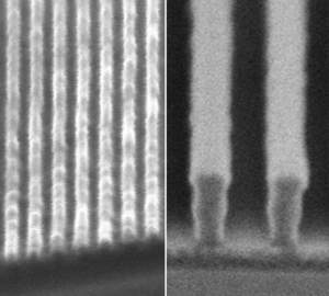 (At left are record-small 29.9-nanometer-wide lines and equally-sized spaces created by IBM scientists – they are less than one-third the size of 90-nm features — at right — now in mass microchip production)
IBM scientists have created the smallest line patterns ever made using deep-ultraviolet optical lithography, the technology currently used to print circuits on chips. The distinct and uniformly spaced ridges are only 29.9 nanometers wide (a nanometer is a billionth of a meter).
The pattern of tiny lines and spaces was created on a lithography test apparatus called NEMO, designed and built at IBM Almaden, using new materials developed in collaboration with JSR Micro. The first technical details will be presented this week (Monday, Feb 20, 2006) at the SPIE Microlithography 2006 conference being held in San Jose, California.
“Our goal is to push optical lithography as far as we can so the industry does not have to move to any expensive alternatives until absolutely necessary,” said Dr. Robert D. Allen, manager of lithography materials at IBM’s Almaden Research Center. “This result is the strongest evidence to date that the industry may have at least seven years of breathing room before any radical changes in chip-making techniques would be needed.”
Microelectronic chips are made by a process called photolithography, which transfers circuit design patterns onto a silicon wafer by projecting a uniform beam of laser light through a shadow mask and then focusing it onto a photosensitive “photoresist” material that coats the silicon wafer. Subsequent development, etching, and materials deposition steps form the circuit features.
The industry has created smaller circuit features — leading to smaller, faster and cheaper electronics — by using ever-shorter wavelengths of light, stronger lenses and by inserting a liquid, currently water, between the final lens and the silicon wafer. It had been thought that this technology would fail below 32 nanometers or so, requiring a shift to X-ray light sources and mirrors rather than lenses to focus the light.